 Excitation to defect-bound band edge states in two-dimensional semiconductors and its effect on carrier transport (二维半导体中缺陷束缚带边态的激发及其对载流子传输的影响)
Dan Wang, Dong Han, Damien West, Nian-Ke Chen, Sheng-Yi Xie, Wei Quan Tian, Vincent Meunier, Shengbai Zhang & Xian-Bin Li
npj Computational Materials 5:8 (2019)
doi:s41524-018-0145-0
Published online:15 January 2019
Abstract| Full Text | PDF OPEN
摘要:杂质离化向半导体带边提供载流子是实现电子器件功能化的关键过程。在二维材料中,由于维度降低和电荷屏蔽减弱,使得杂质电离这一过程变得更加困难。本研究利用第一性原理计算方法,提出了二维半导体掺杂杂质的独特电离过程:载流子只被激发到缺陷束缚带边态,而不是传统三维半导体的自由带边态。这些缺陷束缚带边态的电离能较小,波函数空间分布范围较大。在缺陷密度合适的条件下,载流子可通过这些缺陷束缚带边态传输。
Abstract:The ionization of dopants is a crucial process for electronics, yet it can be unexpectedly difficult in two-dimensional materials due to reduced screening and dimensionality. Using first-principles calculations, here we propose a dopant ionization process for two-dimensional semiconductors where charge carriers are only excited to a set of defect-bound band edge states, rather than to the true band edge states, as is the case in three-dimensions. These defect-bound states have small enough ionization energies but large enough spatial delocalization. With a modest defect density, carriers can transport through band by such states.
Editorial Summary
2D semiconductor: defect bound band edge state(二维半导体:缺陷束缚带边态)
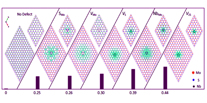
本研究报道了二维半导体存在一种缺陷束缚带边态 (defect-bound band edge, DBBE),对缺陷电离和载流子输运影响显著。来自吉林大学集成光电子国家重点实验室的李贤斌教授领导的团队,以单层MoS2为例,使用第一性原理计算证实了缺陷束缚带边态的存在及其对载流子传输的潜在影响。他们发现形成缺陷束缚带边态的原因是带电缺陷和激发载流子之间存在强束缚作用。该强束缚作用是维度降低的结果,也是二维材料中电荷屏蔽减弱的结果。载流子激发到缺陷束缚带边态所需能量低于形成自由载流子的所需能量,并且位于DBBE态的载流子可以在适当浓度下通过波函数重叠提供传输通道。该传输机制可能是实验观测的二维材料电导的潜在机制。他们的研究揭示了二维半导体中载流子的杂质电离和传输的全新物理图像,对设计新兴纳米电子器件具有重要影响。
There exists a defect-bound band edge (DBBE) state in 2D semiconductors, which has a significant effect on defectionization and carrier transport. A team led by Professor Li Xianbin from the State Key Laboratory of Integrated Optoelectronics of Jilin University used first-principles calculations to verify the existence of DBBE state in single-layer MoS2, an example for 2D semiconductor, and its potential impact on carrier transport. They found that the reason for the formation of DBBE states is strong binding between charged defect and excited carrier. The strong binding is a result of the spatial confinement as well as the reduced screening in 2D materials. The energy required to excite the carrier to DBBE state is lower than the energy required to form the free carrier, and the carriers in DBBE state can provide a transmission channel by wave function overlap at an appropriate concentration. This transport may be a potential mechanism for experimentally observed 2D material conductance. Their research reveals a new physical image of ion ionization and carrier transport in 2D semiconductors, which has an important impact on the design of emerging nanoelectronic devices.

 沪公网安备 31010502006565号